ELECTRONICS
FIB circuit correction
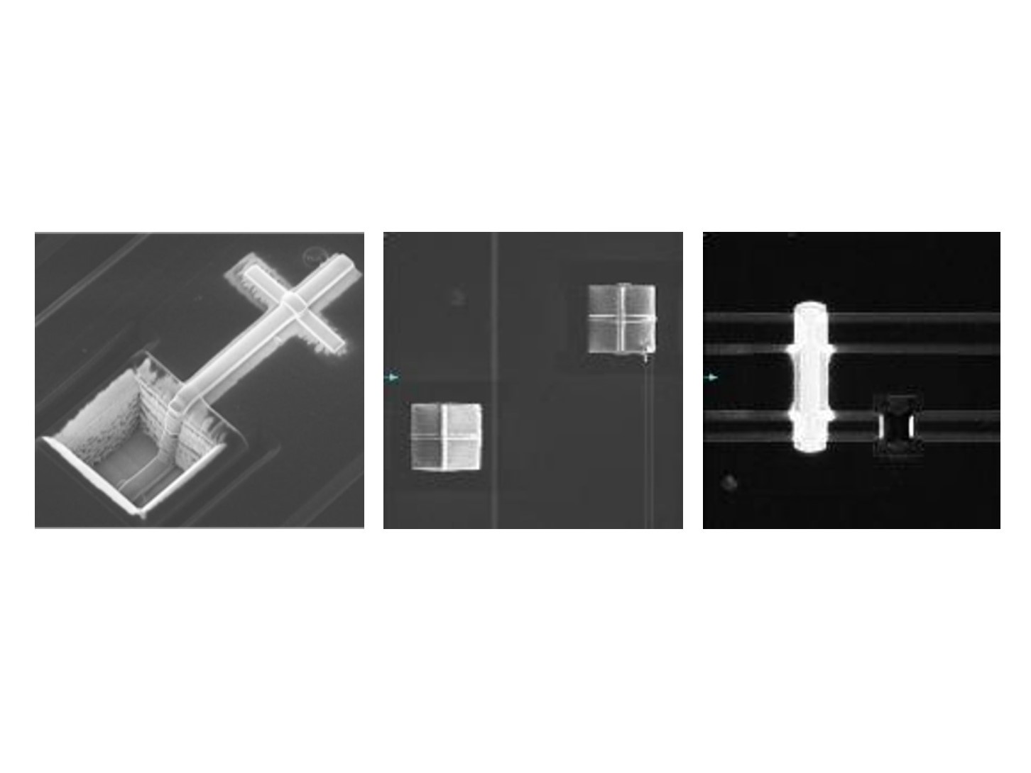
We can offer various kind of FIB service such as circuit correction, defect investigation at circuit design, effect confirmation at mask change and fine image confirmation/cross-section observation with second electron, realizing quick TAT, integrated service (decap~FIB~analysis) , higher skill and technology.
Available for wide range of samples such as PKG products, wafer(up to 12-inch), PCB, bear chip etc.
- Al, Cu(Low-K) wiring process (minimum : 40nm)
- Integrated multiple processes from decap, pre-processing of removal polyimide, up to resin sealing after processing.
- Accurate locational processing by using GDS data overlay system
- PAD make for probes and probe/needle contact are available.
- The FIB place is completely private room and therefore customers can be there to see what are going on.
※GDS data submission may be required.
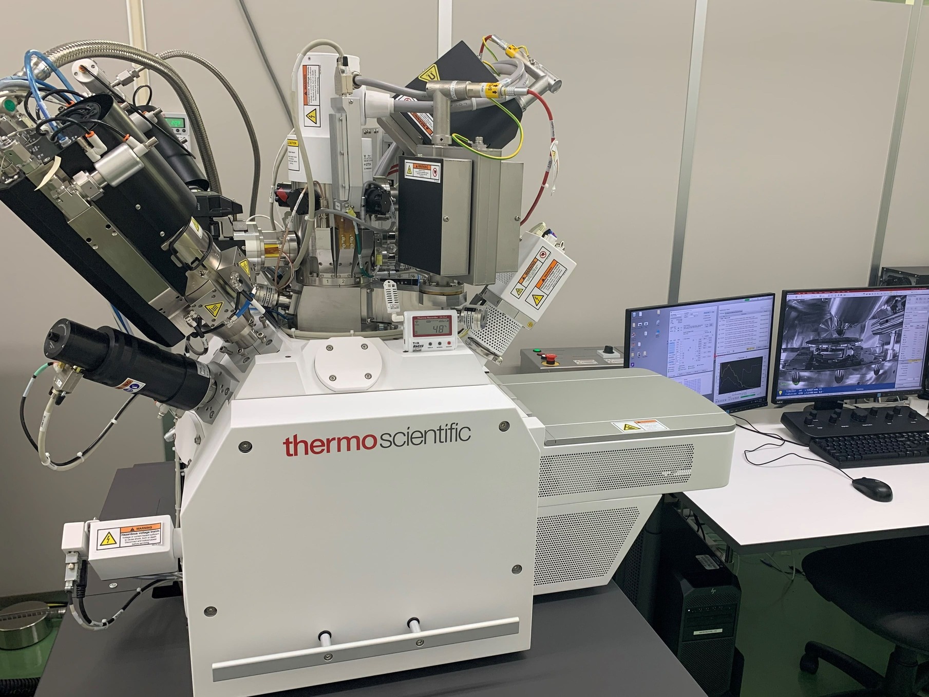
| Maker | Schulumberger/FEI | FEI | |
|---|---|---|---|
| (Shin Yokohama) | (Oita) | ||
| Model | p3x-Ⅰ | p3x-Ⅳ | Centrios |
| Optical function | × | 〇 | × |
| Al wiring etch | 〇 | 〇 | 〇 |
| Oxide film etch | 〇 | 〇 | 〇 |
| Cu etch | 〇 | 〇 | 〇 |
| Polyimide etch | 〇 | 〇 | 〇 |
| Back-side trench | × | 〇 | × |
| Pt depo | 〇 | × | × |
| Mo depo (low resistance) | × | 〇 | × |
| W depo (low resistance) | × | 〇 | × |
| C depo (for cross-section) | × | × | 〇 |
| Oxide film depo | 〇 | 〇 | 〇 |
| WAFER processing | 8inch | × | × |
| Cross-section processing/observation | × | × | 〇 |