ELECTRONICS
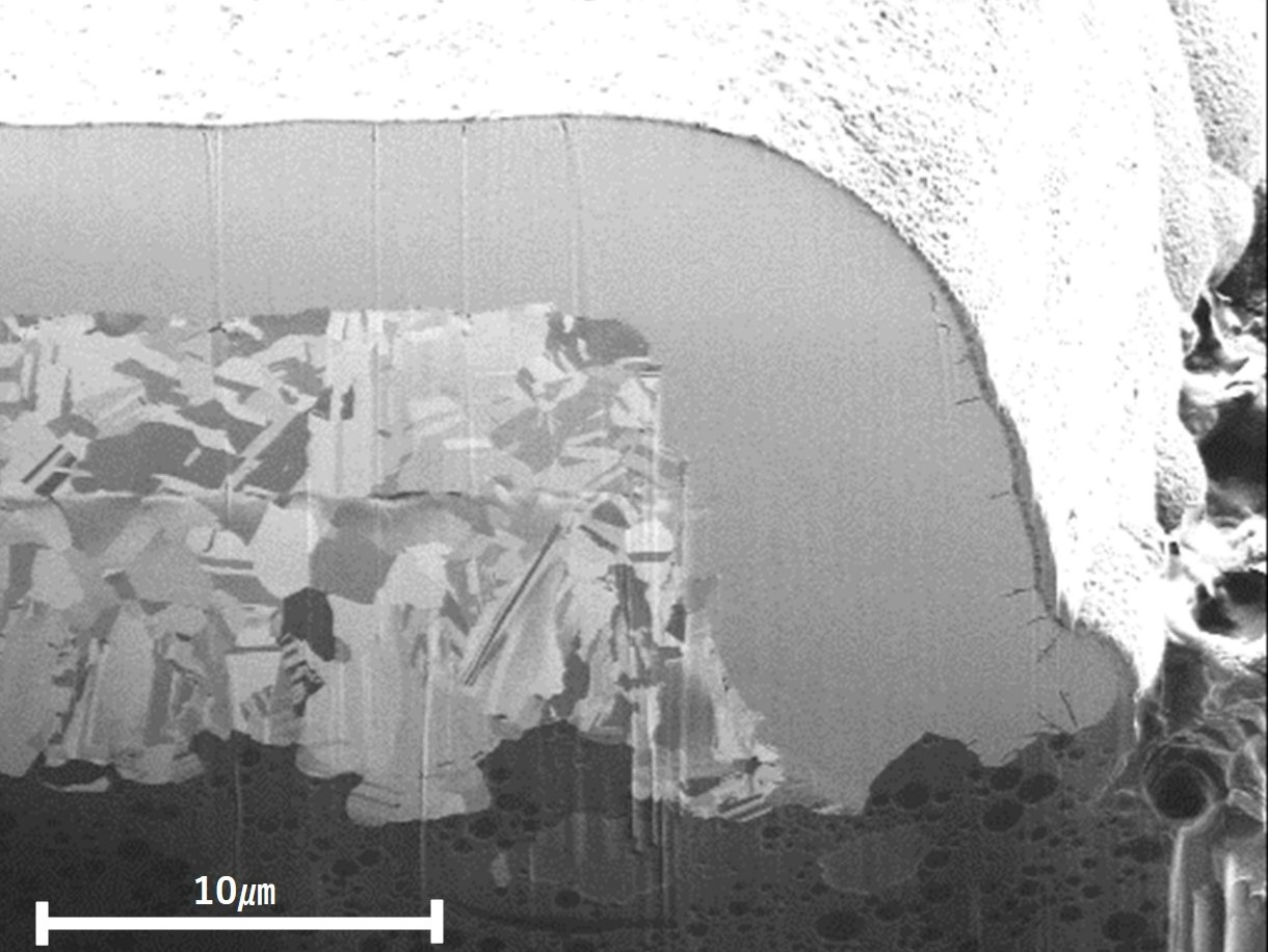
Cross-section FIB analysis
Nano-order observation can be possible by using FIB.
Cross section processing observation
Designated place observation is available by ion beam precious processing.
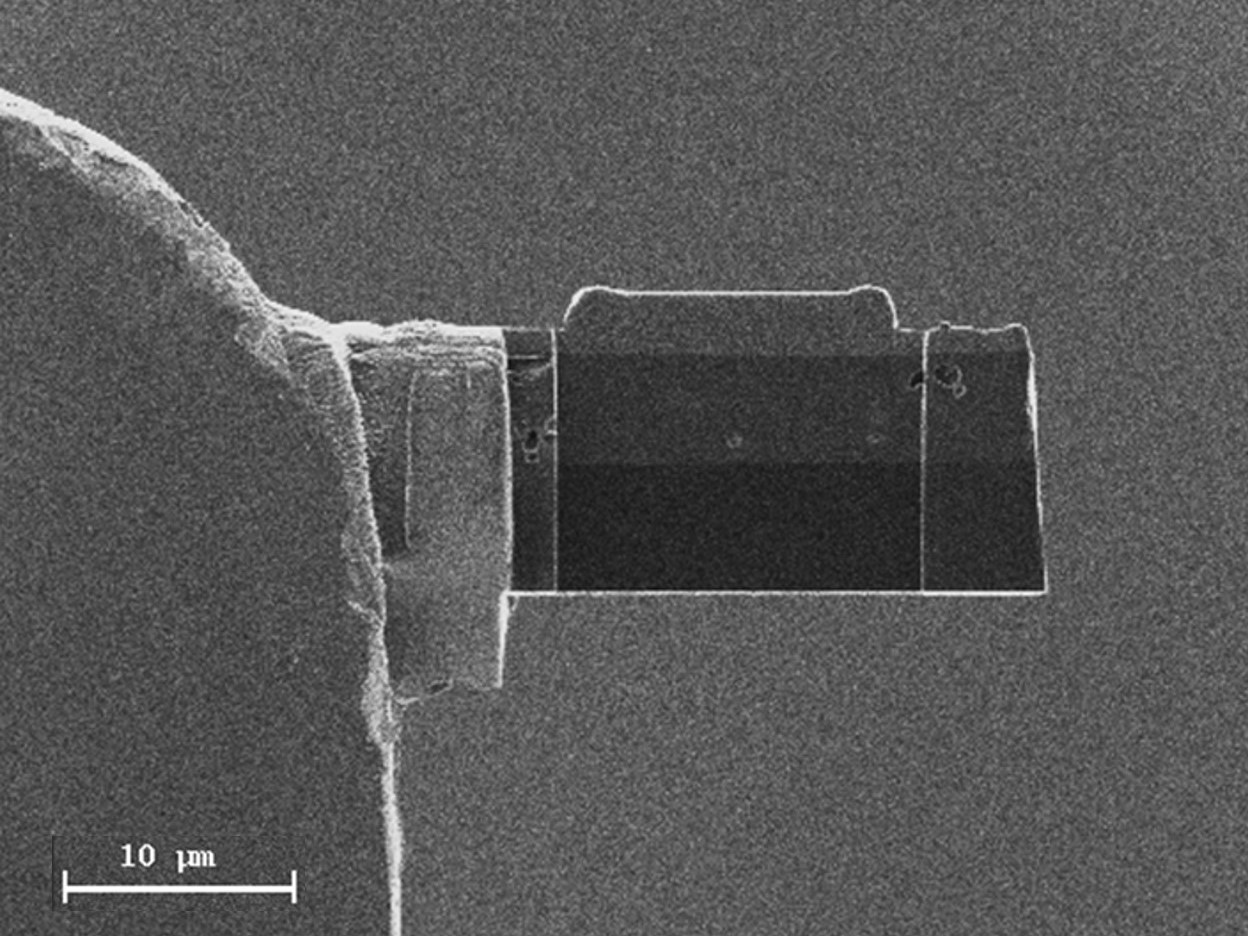
Sample preparation for transmissive electron microscope
25um level micro sample extraction from a sample is possible by using the micro sampling method. Transmissive observation is available with a transmissive electron microscope when designated place thickness is about 100nm.
CMOS structure observation
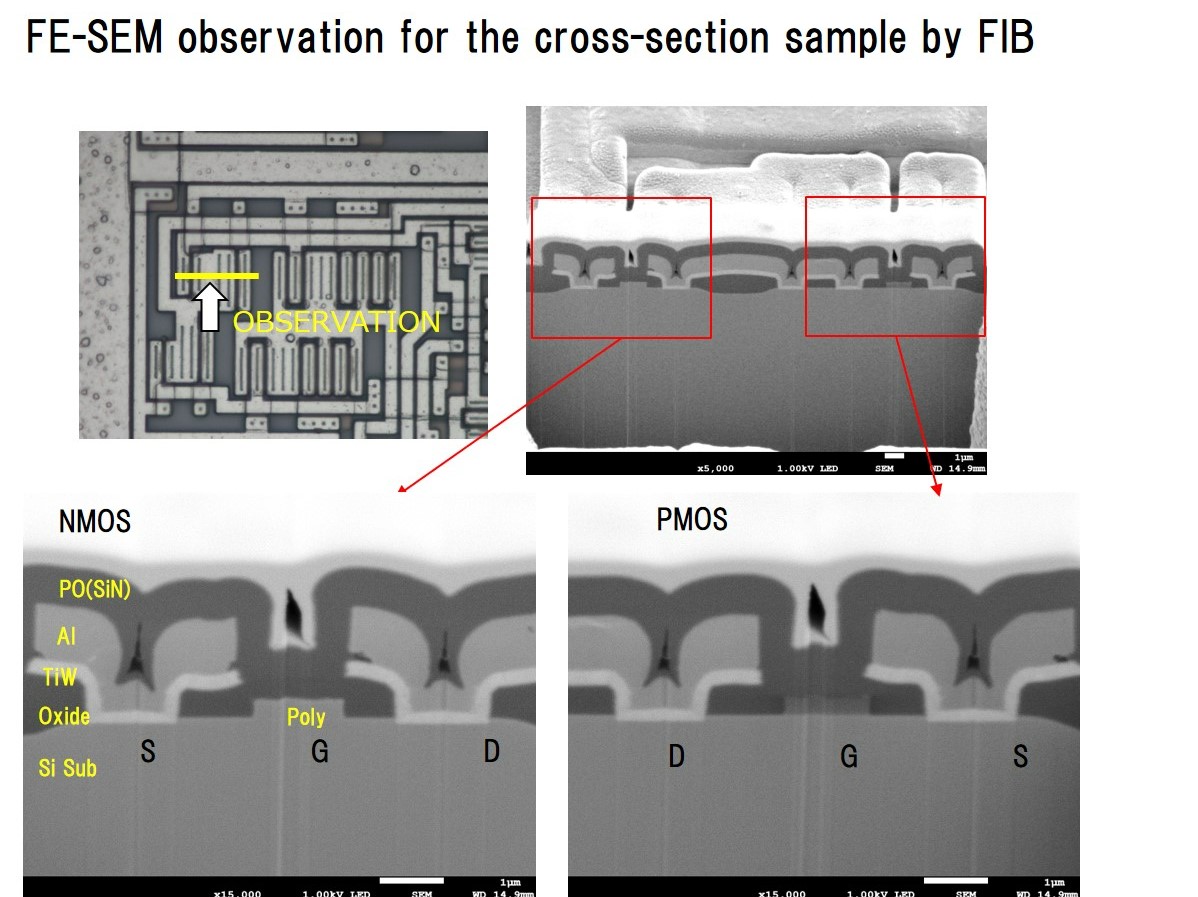
『Dual Beam FIB』that enables electron beam FIB processing along with observation is available. This equipment is the one that can observe FIB processed cross-section just with the SEM and can re-construct several hundred SEM images captured on and off repeated processing and observation, resulting in 3D structure analysis.
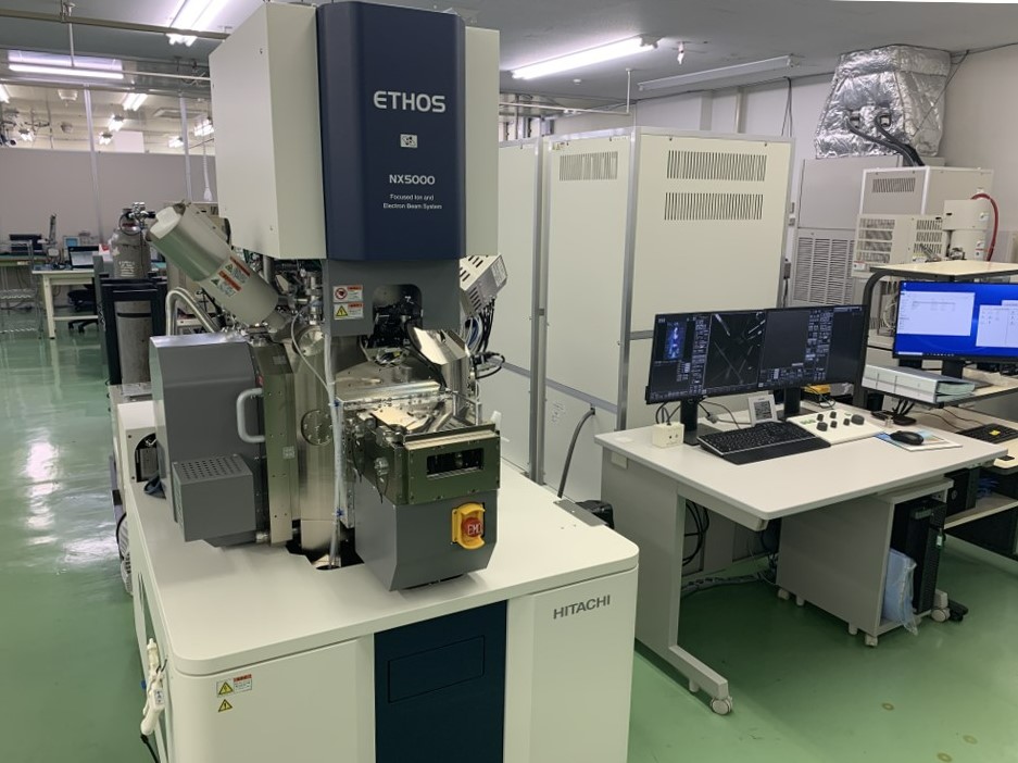
| Part number | FB-2100 | NX-5000 | Centrios |
|---|---|---|---|
| Maker | Hitachi | Hitachi | FEI |
| Acceleration voltage | 10~40KV | 0.1~30KV | 0.5~30KV |
| Max current | 60nA | 100nA | 60nA |
| SIM resolution | 6nm | 4nm | 3.5nm |
| Sample size | 10x10mm | 155x155mm | 30x32mm |
| SEM (electron beam) | × | 〇 | × |
| SIM resolution | Hitachi | Hitachi | FEI |
| Ar/Xe ion beam | ー | 0.7nm@15kV | ー |
| TEM/STEM processing | 〇 | 〇 | × |
| CAD Link | × | × | 〇 |